
Product news
Fineline Stencil Chemistry from Kissel + Wolf
Fineline Stencil Chemistry from Kissel + Wolf
The primary goals of crystalline photovoltaics are to lower cell costs while increasing their efficiency. Screen printing makes a considerable contribution here, as it enables ever-narrower conductive fingers to be achieved at high process speeds on the front side of the solar cell. This and also the miniaturisation of functional prints, for example in electronics, place very high demands on the screen printing stencil. So that the resolution of such fine lines not only occurs in the stencil, but is also able to subsequently function in print, all the stencil production parameters must be perfectly coordinated with each other.
This system comprises several steps, which are shown in Figure 1. With each step, the stencil can be gradually optimised for your own in-house process.
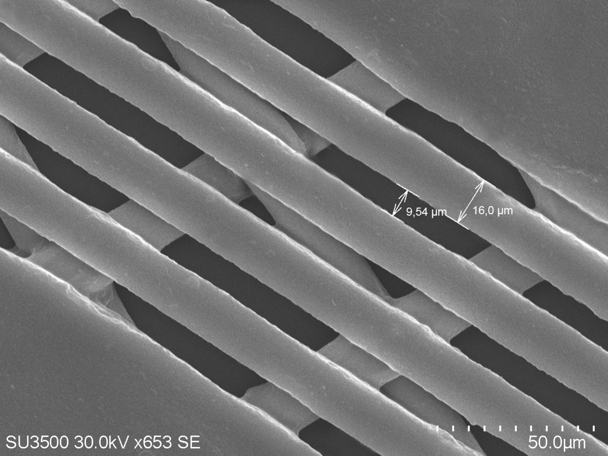
First, a base coating with a high-resolution emulsion should be done. For example, using the highly resistant AZOCOL Z 177 FL or its successor AZOCOL Z 177/1 FL, which, with a higher EOM of approximately 15 μm, can achieve resolutions of up to 20 μm.
When using aggressive solvents or for very high runs, AZOCOL Z 173/1 FL-H is recommended, which can be also be post-hardened and at the same time can generate very high resolution.
Following the emulsion coating, ESTELAN® D 271 TopCoat can be post-coated on the printing side, which further improves the Rz value and protects the screen printing stencil from mechanical attacks during the printing process.
Especially in the solar sector, a uniform topography of the printed line is important so that electricity can flow unhindered.
For this purpose, Kissel + Wolf offers a product called KIWOMIX® RA 1750, which can modify the stencil surface so that the paste release characteristics of the stencil are additionally supported.


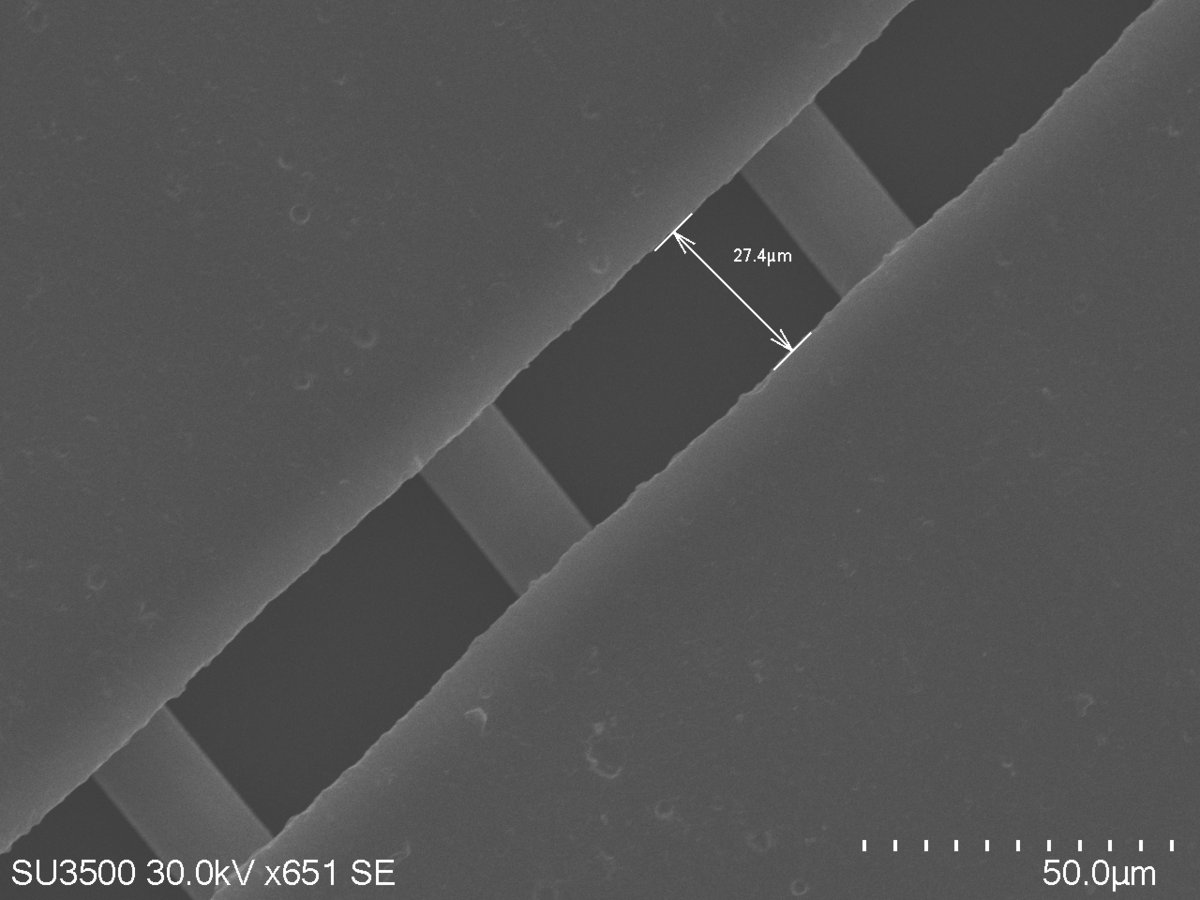
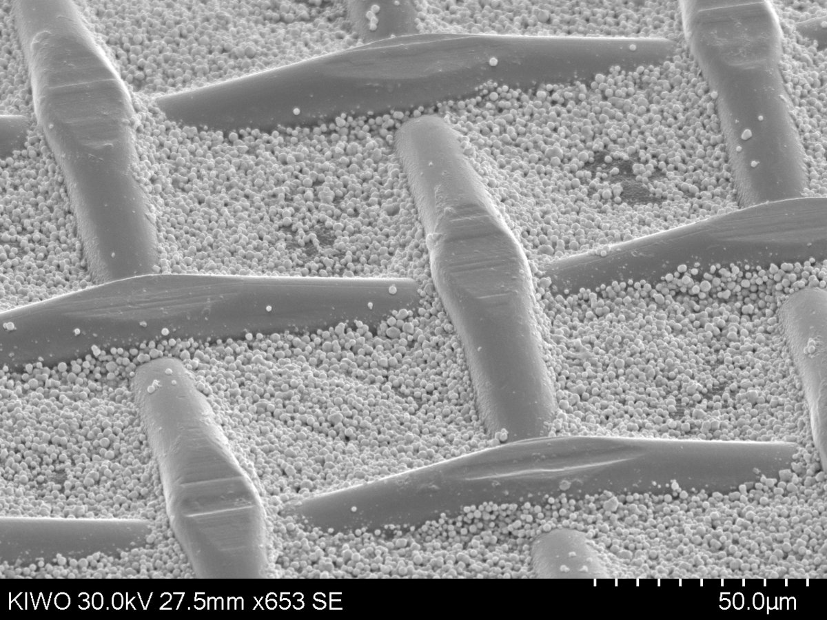
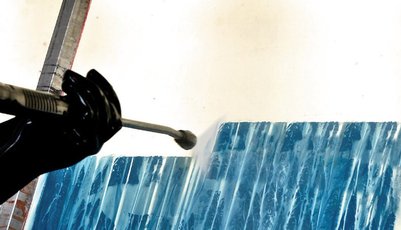
If the resolution required has been generated in the stencil, this does not yet mean that it can be used for printing - the right mesh is also crucial. Mesh is now available with thin threads of 11 µm to eliminate in the best case disruption in the printed line. An increasingly important issue is also the angling of the mesh. Usually 22.5 ° and 30 ° angles are used as standard. The problem with printing is that the lines to be printed run over the knuckle points of the mesh and this can lead to disruption in the printed image.
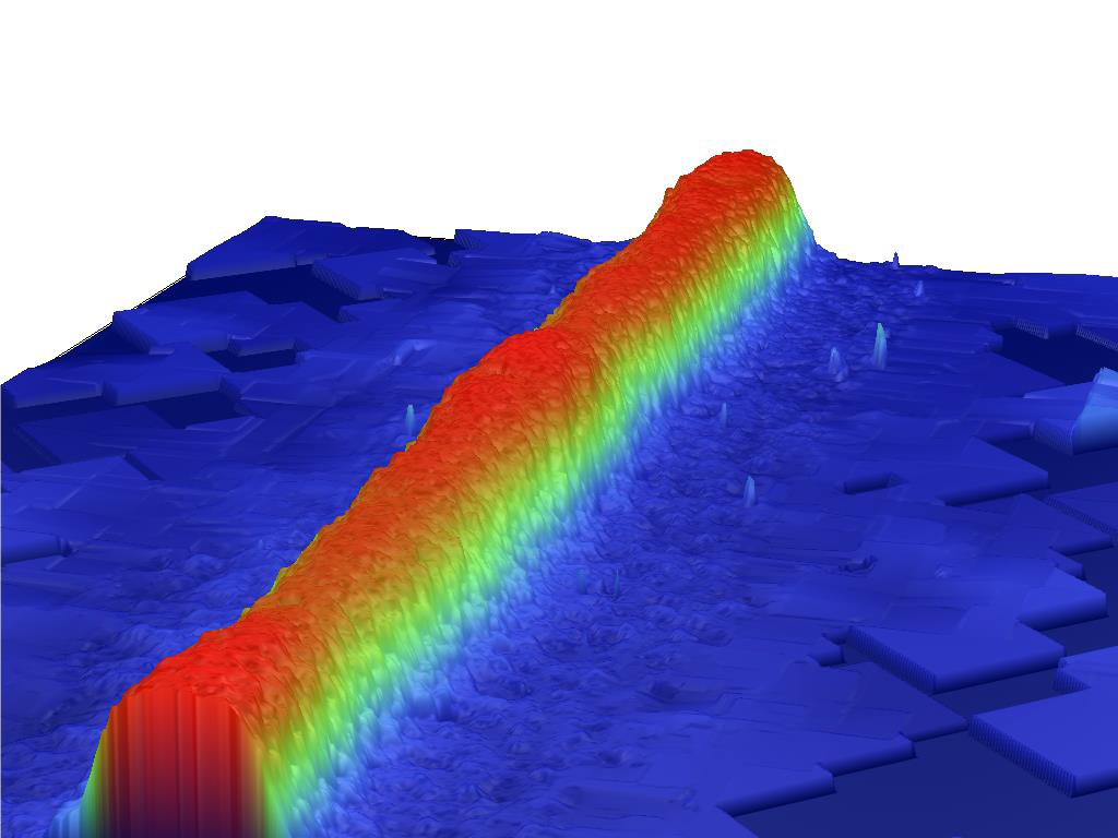
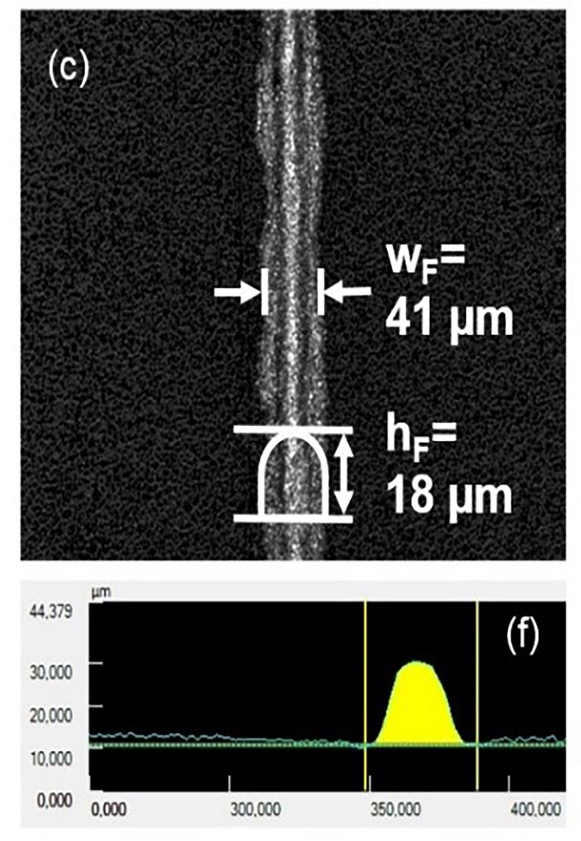
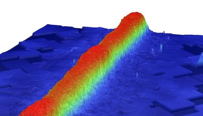
For this reason, zero-degree mesh is being increasingly tested and already also in partial use – in the optimum case, the negative line runs parallel with the threads, so that varying on mesh geometry, no "thick" knuckle points but only a thin weft thread is transverse to the printing channel. This allows significantly better profiles to be printed - both shown in Figure 2.
It should be noted, however, that the demands on the emulsion for these mesh types increase, since reflection characteristics during the exposure process are different than at standard angles.
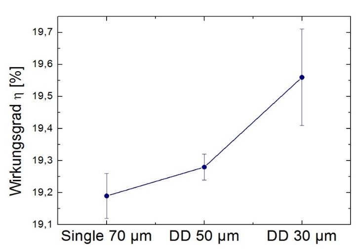
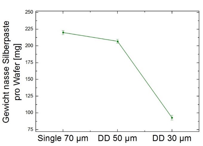
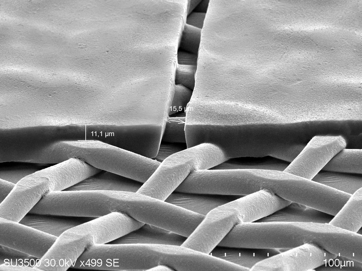
In printing itself, potential defects can be compensated by double printing, resulting in more homogeneous conductive fingers, thus consequently enabling better efficiency to be achieved. The Institute of Photovoltaics (ipv) at the University of Stuttgart used AZOCOL Z 177 FL to test double printing with 30 μm lines. An efficiency increase of 0.37% was achieved compared to the simple printed 70 μm line - as shown in Figure 3. Furthermore, the paste consumption in this printing test was reduced considerably, as shown in Figure 4. If there were still just 225 mg / wafer single-printed at 70 μm lines, clearly less than 100 mg / wafer were required at 30 μm when double printed.
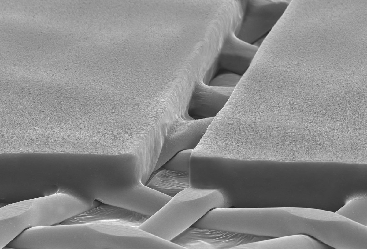
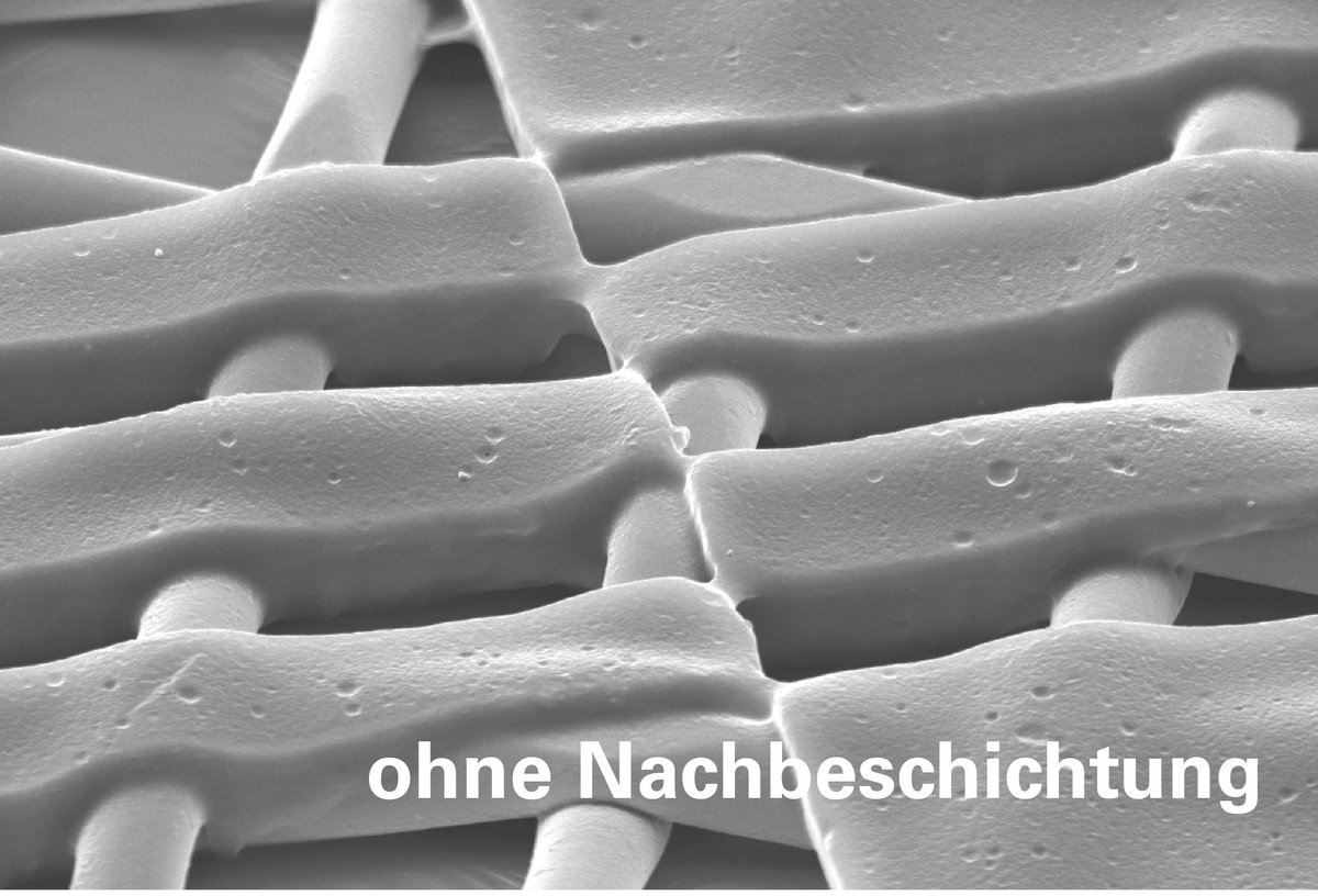
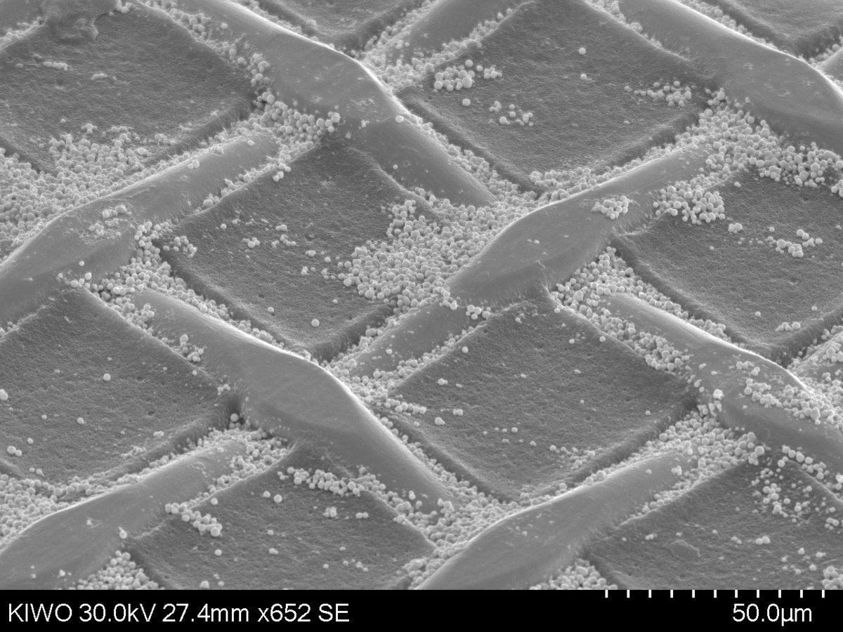
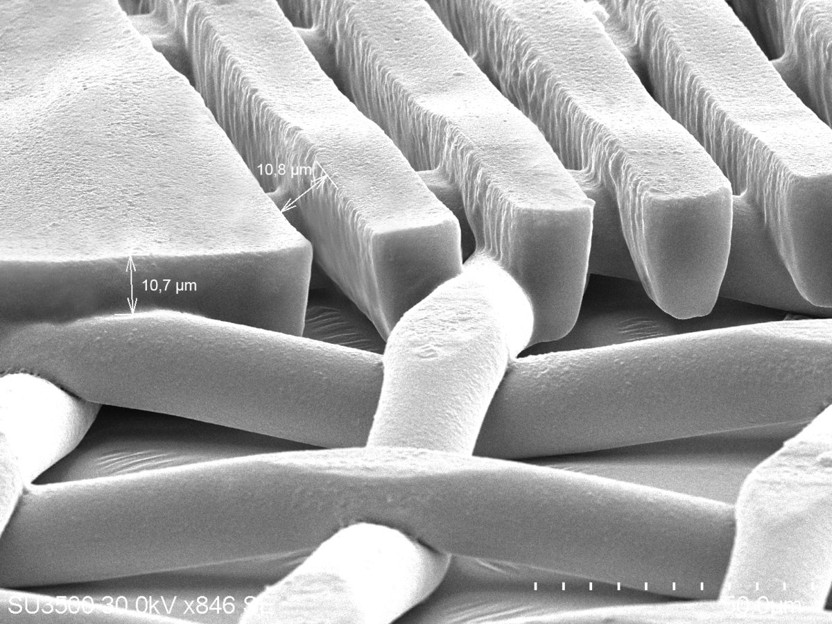
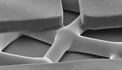
In addition to the stencil chemistry used, it is equally important how it is applied. An example of an optimised stencil technique is shown in Figure 5: The emulsion forms a cuboid effect on the squeegee side in the mesh. The big advantage is that the consumption of paste and associated costs can be greatly reduced. A negative example can be seen on the right-hand side. The emulsion forms a concave structure in the mesh, in which a lot of paste gets stuck.
It becomes clear that these finest lines can only be deposited with great effort on the substrate, but development in terms of resolution is still far from over.
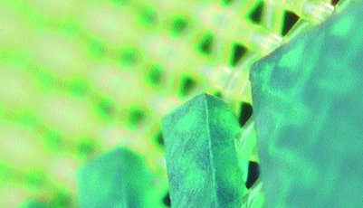
Kissel + Wolf will launch an even higher resolution product in the near future, which can achieve line resolutions of ≤ 15 μm with an EOM ≥ 10 μm. A small preview of this emulsion can be seen in Figure 6.
Read more product news

Read more company news
 New sales responsibility in the screen-printing and textile-printing DACH NL
 Rewarding a long-term partnership
 New distribution agreement
 ![[Translate to English:]](/fileadmin/_processed_/6/2/csm_Mobil_Bild_07f3104336.jpg "[Translate to English:]") Kissel + Wolf appoints distribution partner
Kissel + Wolf appoints distribution partner Kissel + Wolf social engagement 2020
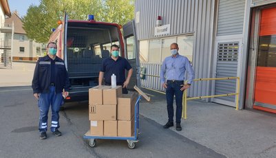 Kissel + Wolf donates disinfectant
![[Translate to English:]](/fileadmin/_processed_/7/8/csm_Kissel_und_Wolf_Spendenaktion_2019_bbbc67feb4.jpg "[Translate to English:]") Kissel + Wolf social engagement 2019
Kissel + Wolf social engagement 2019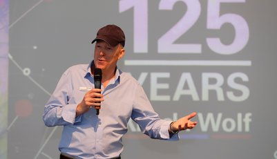 125 years Kissel + Wolf GmbH
 Industrial Screen-Printing Applications
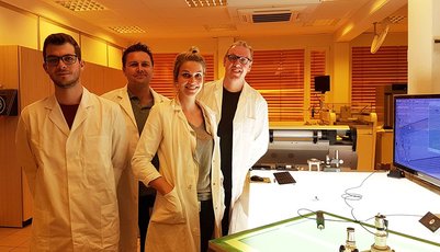 Investments in our Applications Laboratory